COMMUNITY PROJECT: “SHARING LOVE – SUPPORTING CHILDREN IN FLOOD-HIT AREAS OF PHU YEN & GIA LAI”

DỰ ÁN CỘNG ĐỒNG: “CHIA SẺ YÊU THƯƠNG – HƯỚNG VỀ TRẺ EM VÙNG LŨ PHÚ YÊN & GIA LAI”
Vì có những thứ đã bị dòng nước cuốn trôi mà nỗ lực của các em thì không bao giờ mất…
Những ngày qua, lũ dữ đã cuốn đi gần như tất cả:
📌 Sách vở – bút mực – balo mà các em dùng mỗi ngày
📌 Quần áo – dép – áo mưa cho mùa đi học
📌 Và đau lòng hơn, có em đã mất cả người thân trong trận lũ
Trong khi học kỳ sắp kết thúc, kỳ kiểm tra đang đến gần…
Trong khi học kỳ mới chỉ còn ít tuần nữa sẽ bắt đầu…
Trong khi Tết đang đến rất gần, lẽ ra các em được mặc áo mới, giày mới, cầm quyển vở mới…
Nhưng hiện tại, rất nhiều em không còn gì trong tay.
Chúng tôi phát động chương trình quyên góp khẩn:
📚 Sách vở – bút mực – balo – đồ học tập
🧥 Quần áo mới/như mới, áo ấm, dép, áo mưa
🎁 Sữa – bánh – khăn mặt – đồ dùng cá nhân
📌 Thời gian nhận: 1/12/2025-15/12/2025
📌 Địa điểm:
Lớp 11H1-Nhà C Trường THPT Chuyên Hà Nội Amsterdam
Thư viện tầng 1, Tòa 25T1 N05 KĐT Đông Nam Trần Duy Hưng, Yên Hòa, Hà Nội
Mỗi quyển vở gửi đi là một cơ hội để các em tiếp tục học.
Mỗi bộ quần áo là một chút hơi ấm trước Tết.
Mỗi sự chia sẻ của bạn có thể giúp một em nhỏ đứng dậy sau mất mát.
Hãy cùng chúng tôi mang lại cho các em một khởi đầu mới.
Xin cảm ơn tất cả tấm lòng ❤️🙏

COMMUNITY PROJECT: “SHARING LOVE – SUPPORTING CHILDREN IN FLOOD-HIT AREAS OF PHU YEN & GIA LAI”
Because some things may be swept away by the flood, but the efforts of the children never disappear…

In recent days, the devastating floods have taken away almost everything:
📌 Notebooks – pens – backpacks the children use every day
📌 Clothes – sandals – raincoats for their school days
📌 And even more heartbreaking, some children have lost their loved ones in the disaster

While the semester is nearing its end, and exams are approaching…
While the new school term will begin in just a few weeks…
While Tet is coming very soon—when the children should be wearing new clothes, new shoes, holding new notebooks…

But now, so many of them have nothing left.

We are launching an urgent donation drive:
📚 Notebooks – pens – backpacks – school supplies
🧥 New/almost new clothes, warm jackets, sandals, raincoats
🎁 Milk – biscuits – towels – personal items

📌 Donation period: 1/12/2025–15/12/2025
📌 Drop-off locations:
Class 11H1 – Building C, Hanoi–Amsterdam High School for the Gifted
1st Floor Library, 25T1 Building, N05 Urban Area, Dong Nam Tran Duy Hung, Yen Hoa, Hanoi

Each notebook you send is a chance for a child to continue learning.
Each set of clothes is a bit of warmth before Tet.
Each act of kindness can help a child stand up again after their loss.

Let’s join hands to give the children a fresh start.
Thank you for every heartfelt contribution ❤️🙏

Failure Analysis: Water Purifier Circuit

Despite completing the full PCB design workflow in Altium Designer, the final implementation of the Water Purifier control circuit did not achieve the intended functionality. During the testing phase, the circuit failed to maintain stable voltage and current levels required for the purification modules, resulting in incomplete filtration. The output water remained impure and unsafe for use, indicating that the electronic control system was not effectively regulating the purification process.

The main source of failure was traced to insufficient power management and grounding design. Electrical noise interfered with sensor readings and relay operations, causing unstable control signals and irregular pump activation. As a result, the filtration cycle was frequently interrupted, and the purifier could not sustain the necessary operating conditions for proper water treatment.

Additionally, the PCB layout lacked adequate decoupling and shielding, leading to voltage drops across key components. This design flaw, combined with inaccurate sensor calibration, prevented the system from responding accurately to water quality feedback. Even though the schematic and routing were technically valid, the real-world performance exposed critical weaknesses in electrical reliability and system integration.

This failure demonstrated that correct circuit design on software alone does not guarantee functional success in hardware. The team recognized the importance of validating design assumptions, simulating real load conditions, and performing detailed power integrity analysis before production. Although the project did not meet its practical goal, it provided valuable lessons in identifying and understanding failure mechanisms in PCB-based control systems.

Electronic Circuit Design with Altium Designer: Basic Operation, Component Arrangement, and Finalization

1. Objective

The objective of this initial stage was to familiarize our team with the fundamental operations of Altium Designer 24, establish a structured workflow for PCB creation, and develop the preliminary circuit layout for the Water Purifier Project. Throughout these lessons, we aimed to gain hands-on experience in basic tool manipulation, component placement, electrical rule setup, and final board preparation for fabrication.

2. Summary of Learning

We began by learning the essential interface operations in Altium Designer, including project creation, schematic navigation, and fundamental editing commands. This foundation helped us understand the complete workflow from schematic design to PCB layout.

Next, we organized the circuit components, defined electrical connection rules, and routed signal traces to ensure logical connections between modules. Using Altium’s rule management tools, we configured net classes, clearance values, and layer settings to achieve a manufacturable layout. During the final phase, we applied teardrops to strengthen solder joints, performed design rule checks to detect spacing or clearance violations, and added copper pours for improved grounding and current distribution.

3. Application to the Water Purifier Project

In the Water Purifier Project, these tasks were implemented to design the first version of the control circuit board. The schematic included the microcontroller, sensors, relay outputs, and power management sections. The PCB outline was customized to fit within the purifier’s enclosure, with careful attention to connector alignment and mounting hole placement.

The routing process ensured efficient current flow between power and signal lines while minimizing electromagnetic interference. Design rules were applied to maintain safety margins, and copper pours were used to stabilize the ground plane, enhancing electrical performance and reliability of the circuit.

4. Conclusion

Through this stage, our group obtained practical knowledge of PCB design fundamentals, such as schematic-to-board transition, electrical rule configuration, and trace optimization. We also learned the importance of iterative checking and precise layout control. This experience strengthened our understanding of how detailed planning and organized execution contribute to a stable and manufacturable PCB design.

5. Next Step

In the next stage, our team will generate Gerber and drill files, perform final 3D verification, and prepare documentation for PCB manufacturing. We also plan to simulate signal integrity and thermal effects to ensure that the final PCB operates safely and efficiently under real-world conditions.

Electronic Circuit Design with Altium Designer: Board Definition, Teardrop Setup, and Design Rule Check

  1. Objective

The objective of this stage is to finalize the PCB board definition, enhance electrical reliability through teardrop connections, and perform a complete design rule verification. These tasks aim to ensure that the PCB layout is both mechanically optimized and electrically robust before fabrication.

  1. Summary of Learning

Under our teacher’s guidance, the team first redefined the PCB board outline to ensure a compact, manufacturable shape that fits the project’s enclosure precisely. We adjusted the board boundaries to include sufficient space for connectors and mounting holes while maintaining efficient component placement.

Next, we configured teardrops at trace–pad and via–trace junctions. This technique strengthens the copper connections, preventing potential cracking or open circuits during the fabrication and soldering process. Using Altium Designer’s teardrop feature, we applied smooth transitions between traces and pads across the entire design.

Finally, the Design Rule Check (DRC) process was conducted to automatically detect clearance, short-circuit, and width violations. All detected issues were reviewed and corrected to guarantee full compliance with electrical and mechanical design constraints.

  1. Application to the Water Purifier Project

In the Water Purifier Project, this stage was applied to the final control board design. The board shape was redefined to fit perfectly inside the purifier housing, allowing convenient access to connectors and stable mounting. Teardrops were added to reinforce solder joints around the microcontroller, sensor inputs, and power traces — all of which are critical for long-term operation in a humid environment.

The DRC process helped us identify and fix several minor spacing violations, ensuring that high-current traces and sensitive analog signals were properly isolated. This improved both electrical safety and signal accuracy within the purifier system.

  1. Conclusion

Through this stage, our team gained deeper insight into PCB mechanical optimization, teardrop strengthening, and automated design verification. We learned that careful attention to manufacturing details such as pad transitions and clearance checks significantly increases the board’s durability and professional quality. This experience enhanced our confidence in producing reliable PCBs ready for industrial-level fabrication.

  1. Next Step

In the next stage, our group will generate Gerber and drill files, perform final 3D verification, and prepare documentation for PCB manufacturing. We also plan to simulate signal integrity and thermal effects to ensure that the final PCB operates safely and efficiently under real-world

Electronic Circuit Design with Altium Designer: PCB Update, Component Placement, and Routing

  1. Objective

The objective of this research stage is to transition from schematic design to printed circuit board (PCB) layout using Altium Designer under the guidance of our supervising teacher. In this stage, our student research team focuses on updating the schematic to the PCB environment, verifying component integrity, arranging components logically, and routing electrical connections with appropriate trace widths.
These tasks are essential for transforming the conceptual schematic into a manufacturable and functional PCB that ensures electrical reliability and design efficiency.

  1. Summary of Learning

Under our teacher’s supervision, the team first performed the Design → Update PCB Document process to synchronize all schematic components and nets with the PCB layout. We reviewed each component footprint and verified the accuracy of every symbol–footprint link to avoid design mismatches.

Next, we practiced strategic component placement, considering signal flow, mechanical constraints, and ease of routing to achieve a compact and logical layout.

In the routing process, we defined trace widths based on current requirements and signal type, ensuring full compliance with design rules. Using Altium Designer’s interactive routing and clearance verification tools, we completed all electrical connections while minimizing crosstalk and maintaining a clean, organized routing structure.

This stage helped our group understand the importance of systematic layout design and accurate rule management in building a reliable PCB.

  1. Application to the Water Purifier Project

In our Water Purifier Project, the knowledge gained from this stage was applied to the control circuit board design. After updating the schematic to PCB, we placed the main components—including the microcontroller, power regulators, and sensors—to optimize signal flow between the control and measurement sections.

The PCB outline was designed according to the 3D mechanical model to ensure proper fitting inside the water purifier enclosure. Trace widths were categorized: wide traces for power supply lines, medium widths for control signals, and narrow traces for sensor inputs.

Routing was performed using both manual and auto-routing tools to ensure stable signal transmission. The final layout resulted in a functional, organized PCB ready for fabrication and testing.

  1. Conclusion

This stage strengthened our team’s understanding of PCB layout design and its real-world application in Altium Designer. Through this guided learning process, we successfully connected theoretical schematic design to practical PCB implementation.
The experience also highlighted how careful layout planning and adherence to design rules can improve electrical performance, reduce interference, and enhance manufacturability. This research stage represents a valuable step in our journey toward mastering electronic hardware design.

  1. Next Step

In the next stage, our team—under the continued guidance of our teacher—will perform Design Rule Checks (DRC), generate Gerber files, and prepare the final PCB documentation for manufacturing. We also plan to conduct thermal and electrical simulations to verify the PCB’s performance before sending it for fabrication.

Electronic Circuit Design with Altium Designer: Wire Labeling, Component Editing, and Annotation

  1. Objective
    The objective of this stage is to enhance schematic clarity and accuracy in Altium Designer by labeling electrical wires, editing component names and values, and assigning proper sequence numbers to all components. These tasks are essential for developing a well-organized and professional schematic that supports the following stages of PCB design in our group’s scientific research project under instructor supervision.
  2. Summary of Learning
    During this phase, our team practiced assigning net labels to wires to clearly define signal connections and prevent confusion between different circuits. We also learned to modify component names and values to accurately reflect their specifications, such as resistor and capacitor ratings. Finally, we used the annotation function to automatically number all components in a logical order. Through these operations, our group gained a deeper understanding of how consistent labeling and naming conventions can improve schematic readability and debugging efficiency.
  3. Application to Water Purifier Project
    In our Water Purifier Project, these skills were applied to the control circuit schematic. Each signal line was labeled according to its function, such as power, ground, and sensor connections. The components on the control board— including the microcontroller unit, transistors, and sensors—were carefully renamed and numbered to match the Bill of Materials (BOM). This process ensured accuracy and consistency in the later PCB layout and assembly stages.
  4. Conclusion
    This stage strengthened our team’s understanding of schematic organization principles in Altium Designer. By applying systematic wire labeling, parameter editing, and component annotation, we built a professional and logically structured schematic. These practices are crucial in large-scale electronic designs, helping to reduce potential errors and enhance collaboration between the design and manufacturing teams.
  5. Next Step
    In the next stage, our group will continue by establishing detailed electrical connections between components, simulating circuit performance, and preparing for the PCB layout process to verify that the schematic functions correctly in real-world operation.

Electronic Circuit Design Fundamentals in Altium Designer: Installation, Workspace Setup, and Library Configuration

Electronic Circuit Design Fundamentals in Altium Designer: Installation, Workspace Setup, and Library Configuration

  1. Objective

The objective of this stage is to develop a foundational understanding of electronic circuit design using Altium Designer. This part focuses on installing the software, setting up component libraries, and learning essential operations and shortcuts for managing schematic projects efficiently.
Our team aims to build a complete and functional design environment for developing the electronic control system of the Water Purifier Project, under the guidance of our instructor.

  1. Summary of Learning

During this phase, our team learned how to download, install, and activate Altium Designer. We practiced configuring the workspace to create a comfortable and efficient working environment. We also installed and organized component libraries, which provide access to common electronic parts such as resistors, capacitors, diodes, and integrated circuits (ICs).

Through the introductory practice (P1), we explored the user interface, identified key design panels, and used keyboard shortcuts to improve design efficiency. We also learned how to create new schematic projects, name and organize files systematically, and prepare folders for future PCB development.

These experiences gave the team a clear understanding of the software structure, workflow for project creation, and the importance of proper library configuration in electronic design.

  1. Application to Water Purifier Project

In the Water Purifier Project, our team applied these skills to set up the electronic control system design environment.
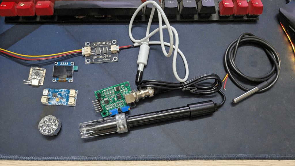
We installed and configured component libraries for the project’s sensor modules, microcontroller, and power management circuits. Then, we created a dedicated Altium project for the purifier’s control board, ensuring clear folder organization for both schematic and PCB files.

This preparation ensures that all future circuit designs will be consistent, accurate, and ready for integration with the mechanical structure previously modeled in SolidWorks.

  1. Conclusion

This stage provided our team with a strong foundation in using Altium Designer. We gained confidence in installing the software, customizing the workspace, and managing libraries — essential skills for professional PCB design.
The knowledge from this phase effectively bridges the gap between the mechanical design phase (SolidWorks) and the electronic design phase (Altium Designer) of the Water Purifier Project, enabling smooth integration in the final prototype.

  1. Next Step

In the next stage, our team will begin schematic drawing and circuit design, connecting sensors, control units, and power components. This marks the first step toward building the functional electronic system of the Water Purifier, preparing for PCB layout and full system integration.

Fundamental 3D Modeling in SolidWorks: Extrude and Revolve Features

    1. Objective

    The objective of this stage is to build a solid foundation in 3D modeling using the Extrude and Revolve features in SolidWorks. This study focuses on converting 2D sketches into precise 3D geometries, understanding the geometric logic behind each tool, and applying these features to create components with real mechanical and engineering value under the guidance of our supervising teacher.

    2. Summary of Learning

    During this research stage, our team learned how to transform 2D sketches into detailed 3D models using the Extrude and Revolve commands.

    • The Extrude feature allows sketches to extend along a specified direction, generating solid bodies such as blocks, plates, or brackets. It provides full control over extrusion depth, direction, and end conditions to achieve precise geometry.
    • The Revolve feature creates rotationally symmetric parts by revolving a sketch around a defined axis—ideal for designing circular or conical components like bottles, pulleys, shafts, and pipes.

    Through multiple practice exercises, our team developed a deeper understanding of sketch preparation, geometric constraints, and feature combination to form accurate models. These activities significantly enhanced our spatial visualization and comprehension of how 2D geometry evolves into complex 3D structures.

    3. Application to Water Purifier Design

    In the Eco Filter Project, we applied these modeling tools to create key components of the portable water purifier:

    • Extrude was used to construct the main body, base plates, and filter casings with precise wall thicknesses.
    • Revolve was used to form cylindrical and conical parts such as filter housings and pipe connectors.

    Using these features ensured consistency, dimensional accuracy, and realistic mechanical fitting between components. This stage also laid the groundwork for future assembly and motion simulation processes by producing structurally sound 3D parts ready for integration.

    4. Conclusion

    This stage established our team’s essential 3D modeling skills in SolidWorks through the use of Extrude and Revolve. By mastering these core tools, we gained a clearer understanding of how 2D sketches develop into mechanical components and how these operations serve as the foundation for advanced design. The process strengthened our precision, spatial reasoning, and confidence in digital modeling—key abilities for developing efficient and reliable engineering products.

    5. Next Step

    In the next phase, our team will explore Cut Extrude, Fillet, and Chamfer tools to refine part details, enhance functionality, and improve aesthetics before proceeding to the assembly stage of the purifier model.

    Advanced Assembly and Technical Drawing in SolidWorksIntegration of Basic and Advanced Mates, Assembly Creation, and Drawing Documentation

      1. Objective

      The objective of this research stage is to develop comprehensive skills in assembling 3D mechanical components and producing technical assembly drawings in SolidWorks. This study, conducted under the guidance of our supervising teacher, focuses on applying both basic and advanced Mate features to enhance mechanical precision, simulate realistic motion between parts, and generate professional 2D documentation for manufacturing and analysis.

      2. Summary of Learning

      Throughout this stage, our team gained a solid understanding of the complete assembly workflow in SolidWorks.

      • Using basic Mate commands such as Coincident, Parallel, Concentric, and Distance, we learned to position and constrain parts accurately, ensuring correct spatial alignment and realistic mechanical behavior. These constraints also helped us detect potential interferences and improve overall design reliability.
      • We then explored advanced Mate tools, including Width, Symmetric, Path, and Limit Mates. These functions enabled dynamic mechanical simulations, replicating real-world movements such as sliding, rotation, and restricted motion between shafts, gears, and structural parts. Through these exercises, our team gained deeper insight into kinematic relationships and motion dependencies in complex mechanical systems.
      • In addition, we learned to create and manage assembly drawings, incorporating exploded views, Bill of Materials (BOM), and annotations. We practiced defining section views and detailed callouts to clearly illustrate component structures and assembly procedures.

      3. Application to Water Purifier Design

      In the Eco Filter Project, these assembly and drawing tools were directly applied to our portable water purifier prototype.

      • Basic Mates were used to align key components such as filter casings, inlet and outlet tubes, and the pump housing with precision.
      • Advanced Mates simulated realistic motion between internal filters, connecting pipes, and mechanical joints to test fit and function before fabrication.
      • The assembly drawings included detailed exploded views showing the relative positions of subcomponents, while the BOM table listed each part’s name, quantity, and material, providing complete documentation for production and maintenance.

      4. Conclusion

      This research stage significantly strengthened our ability to transition from independent 3D parts to a fully functional mechanical assembly. We mastered the use of Mates, motion simulation, and technical drawing documentation—core competencies in professional mechanical design. The process enhanced our precision, problem-solving skills, and spatial visualization, forming a strong foundation for real-world engineering applications.

      5. Next Step

      In the next phase, our team will advance to Simulation and Rendering modules in SolidWorks. These tools will be applied to analyze mechanical motion, evaluate stress distribution during operation, and create photorealistic renderings of the portable water purifier model for presentation and performance evaluation.

        Advanced SolidWorks Modules: Swept, Lofted, Shell, Rib, Wrap, Pattern, Assembly, and Drawing

        1. Objective

        The objective of this stage is to apply and integrate advanced part modeling and assembly techniques in SolidWorks—including Swept, Lofted, Shell, Rib, Wrap, Pattern, Assembly, and Drawing tools—to design, assemble, and document a complete 3D model of a portable water purifier. This stage aims to achieve both functional precision and professional presentation under the guidance of our supervising teacher.

        2. Summary of Learning

        Throughout this research stage, our team explored a range of advanced modeling and assembly features in SolidWorks.

        • The Swept and Lofted commands were used to create complex geometries with smooth transitions and varying cross-sections, which are essential for designing curved connectors and streamlined fluid paths.
        • The Shell and Rib tools helped reduce material usage while maintaining structural strength, allowing us to design lightweight yet durable housings.
        • The Wrap feature was applied to project sketches onto curved surfaces, enabling the creation of engraved logos and decorative labels.
        • Pattern tools (Linear and Circular) were used to efficiently replicate repeated elements such as holes, fins, and ribs, ensuring symmetry and design consistency.

        In the Assembly environment, we practiced combining all designed components using mates such as coincident, concentric, and distance to ensure precise alignment and realistic motion. Finally, in the Drawing module, our team generated 2D technical drawings from the 3D models, including dimensions, annotations, and exploded views for manufacturing documentation and presentation purposes.

        3. Application to Water Purifier Design

        Each advanced modeling tool was systematically applied to the portable purifier design.

        • Swept and Lofted features were utilized for internal flow tubes and filter housings.
        • Shell and Rib improved the casing’s strength-to-weight ratio and reinforced thin-walled structures.
        • Wrap added engraved labeling and aesthetic detailing, while Pattern commands allowed efficient duplication of holes, vents, and screws.

        During the Assembly stage, all parts were precisely aligned and mated to form a complete prototype, ensuring smooth fit and interaction between the filters, connecting pipes, and outer frame. The Drawing environment provided professional 2D blueprints with full dimensions, annotations, and exploded views, serving as essential documentation for real-world manufacturing and assembly.

        4. Conclusion

        By mastering advanced modeling, assembly, and documentation tools, our team successfully created a detailed, manufacturable 3D prototype of the portable water purifier. The integration of part modeling, mechanical assembly, and engineering drawing not only enhanced technical accuracy but also reflected professional standards in product design and presentation. This stage represents a major milestone in the Eco Filter Project, demonstrating the team’s ability to move from concept to near-production readiness.

        5. Next Step

        The next research phase will focus on Rendering and Simulation in SolidWorks.
        → Our team will analyze fluid flow, evaluate structural strength, and create realistic visual renderings of the water purifier to assess both functional performance and presentation quality before prototype fabrication.